- Sony Semiconductor quietly listed the Nikon Z6III’s IMX820 sensor on their product page — and it’s the only consumer camera sensor tagged with CoW BI (Chip-on-Wafer, Back-Illuminated) technology.
- CoW BI uses Copper-to-Copper (Cu-Cu) hybrid bonding to stack pre-tested logic chips directly onto the pixel wafer, enabling radical readout speeds, flexible chip sizing, and on-sensor AI processing.
- The Nikon Z6III already benefits: 3.5× faster readout than the Z6II, 120fps burst, and 6K60 internal RAW. This technology is the foundation for next-gen sensors.
- With a major new Sony E-mount camera confirmed for May and A7R VI rumors pointing to an 80MP stacked sensor, CoW BI could unlock full-frame global shutters and 8K+ video in the near future.
When Sony Semiconductor Solutions quietly updated their consumer camera image sensor product page, most people scrolled past. But one sharp-eyed detail — first spotted by NikonEye — sent ripples through the camera tech community: the Nikon Z6III’s 24MP IMX820 sensor is now publicly listed, and it carries a technology designation that no other consumer camera sensor on the page shares.
That designation is CoW BI — Chip-on-Wafer, Back-Illuminated. And understanding what it means reveals a great deal about where Sony (and by extension, every camera brand that uses Sony sensors) is heading next.
What Sony Quietly Published
Sony’s semiconductor division maintains a public product catalog of their image sensors for camera manufacturers. The listing is dry — model numbers, pixel counts, interface specs. But the newly added IMX820 entry stands out in one critical column: Technology.
Every other full-frame sensor on the page — the IMX455 (61MP, used in Sony A7R IV/V), the IMX410 (24MP, used in Sony A7 III), the IMX366 (44MP) — is listed simply as “BI” (Back-Illuminated). Some smaller sensors carry “Stacked BI” designations.
The IMX820? It’s the only one labeled “CoW BI.” That’s not just a minor manufacturing variation. It represents a fundamental shift in how Sony builds camera sensors.
CoW vs. WoW: The Bonding Revolution Explained
To understand why CoW BI matters, you need to know how stacked sensors are currently assembled.
Traditional stacked sensors use WoW (Wafer-on-Wafer) bonding. Sony takes an entire silicon wafer covered in pixel arrays and permanently presses it against another entire wafer covered in logic circuits. Then they dice both bonded wafers into individual sensor chips. This is how sensors like the one in the Sony A9 III (with its global shutter) are manufactured.
CoW (Chip-on-Wafer) does something different. Sony first dices one of the wafers into individual logic chips, tests each chip to confirm it works, and then bonds only the verified good chips onto the larger pixel wafer using microscopic Copper-to-Copper (Cu-Cu) hybrid bonding.
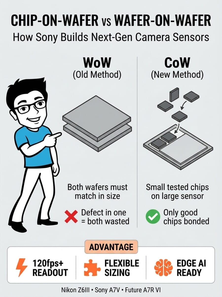
The difference sounds subtle but it has massive implications for camera technology.
Why CoW BI Is a Big Deal for Cameras
Moving from traditional stacking to Chip-on-Wafer bonding gives Sony four key advantages that directly impact the cameras you shoot with:
Flexible Size Matching
In full-frame sensors, the pixel array is physically large — about 36×24mm. With WoW bonding, the logic circuit wafer bonded beneath it has to be equally large, even if the actual logic circuitry only needs a fraction of that space. That wastes expensive silicon.
CoW eliminates this constraint. Sony can attach a small, purpose-built logic chip to a large pixel array. This means they can use the most advanced (and expensive) fabrication process for the logic chip without paying for a massive die that’s mostly empty space.
Known Good Die = Higher Yields
With WoW bonding, if a single logic chip on the bottom wafer is defective, it ruins the perfectly good pixel sensor bonded above it. Both are scrapped. Since defect rates compound across two full wafers, yield losses can be significant.
CoW uses what the semiconductor industry calls “Known Good Die” — Sony tests each individual logic chip before bonding. Only chips that pass get attached to the pixel wafer. This drastically reduces manufacturing waste and lowers the per-sensor cost.
Radical Readout Speeds
CoW bonding allows Sony to optimally position specialized functional chips — like advanced A/D converters or high-speed DRAM — directly on top of the pixel wafer using Cu-Cu hybrid bonding. This creates thousands of microscopic copper-to-copper connections that enable massive parallel data transfer.
This is the technology behind Sony’s 127-megapixel IMX661 industrial sensor, which achieves a completely distortion-free global shutter. It’s also how the Nikon Z6III achieves its 3.5× faster readout compared to the Z6II — fast enough for 120fps burst shooting and 6K60 internal RAW video.
On-Sensor AI Processing
Because CoW bonds individual chips rather than entire wafers, Sony can stack specialized AI processors directly onto the sensor. These chips can analyze image data — detecting subjects, adjusting exposure, running noise reduction — before the data even reaches the camera’s main processor.
Sony has already published research papers on this approach. Combined with the BIONZ XR2 processor expected in upcoming cameras, on-sensor AI could enable real-time computational photography features that current cameras simply can’t manage.
The Nikon Z6III Connection
The Nikon Z6III, launched in June 2024 at $2,499, was the world’s first camera with a “partially stacked” sensor. That description confused many photographers at launch. Now, Sony’s product page fills in the technical picture.
The IMX820’s CoW BI designation explains the “partial” stacking. Rather than bonding two full wafers together (which would make it “fully stacked” like the Z8’s sensor), Sony bonded individual pre-tested logic chips onto the pixel wafer. The result is a sensor that delivers many of the speed benefits of full stacking — 120fps burst, 20fps RAW, 1/16000s electronic shutter — at a significantly lower manufacturing cost.
Sony Alpha Rumors notes that the same sensor is also used in the Panasonic Lumix S1II. Interestingly, the 33MP partially stacked sensor from the Sony A7V is not listed on the public product page — reportedly because Sony is keeping it exclusive to the Alpha line until 2027.
What This Means for the Rumored Sony A7R VI
Here’s where things get really interesting. Sony Alpha Rumors has confirmed that a major new Sony full-frame E-mount camera is coming in May. The leading candidate: the Sony A7R VI, with leaked specs suggesting an 80MP stacked sensor, 30fps RAW bursts, and 16 stops of dynamic range.
If Sony is now publicly acknowledging CoW BI as a production technology for consumer cameras, it’s reasonable to assume the A7R VI’s rumored sensor would also use this approach — likely an evolution of it. Consider the implications:
- 80MP with fast readout: CoW’s flexible size matching means Sony can pair a massive 80MP pixel array with a compact, high-speed logic chip fabricated on a cutting-edge process node. WoW bonding would make an 80MP stacked sensor prohibitively expensive.
- 30fps at full resolution: The Cu-Cu hybrid bonding’s parallel data transfer is what makes high-speed readout of large sensors viable. Reading 80 million pixels 30 times per second generates roughly 57.6 Gbps of raw data — you need thousands of simultaneous copper connections to move that fast.
- Path to full-frame global shutter: Sony already demonstrated this with the A9 III’s smaller sensor. CoW BI makes scaling global shutter technology to higher resolutions economically viable by eliminating wafer size constraints.
- On-sensor AI autofocus: The A7R VI is rumored to include AI-powered autofocus tracking. With CoW-enabled on-sensor processing, subject detection could happen at the sensor level with near-zero latency.
The Bigger Picture: Sony’s Sensor Roadmap
Sony Semiconductor Solutions has been publishing research papers on Cu-Cu hybrid bonding since at least 2017. Their recent work on 2.0μm pitch CoW bonding — meaning copper connections spaced just two-thousandths of a millimeter apart — demonstrates they’re pushing the technology far beyond what’s currently deployed in consumer cameras.
For perspective, the IMX820 in the Z6III likely uses a relatively relaxed bonding pitch. As Sony shrinks the pitch in future sensors, the density of chip-to-wafer connections increases exponentially, enabling:
- Three-layer stacking: Pixel array + logic + DRAM, all bonded with Cu-Cu connections (Sony has published research on this exact configuration)
- 8K120p video readout: Full-frame sensors fast enough to read 33+ megapixels at 120fps for 8K slow-motion
- Consumer global shutters above 50MP: The holy grail for high-resolution cameras — zero rolling shutter distortion at any resolution
Canon has its own stacking technology (as seen in the leaked Canon EOS R7 Mark II sensor), but Sony’s public acknowledgment of CoW BI suggests they’re at least one generation ahead in packaging technology.
What Photographers Should Take Away
If you’re not a semiconductor engineer, here’s the practical summary:
- Sensor technology is advancing faster than camera bodies. The IMX820’s CoW BI designation proves Sony is deploying advanced packaging technology that was previously confined to industrial and research sensors.
- The Z6III was a proof of concept. Its “partially stacked” sensor was the first consumer deployment of CoW BI. Future cameras will use more aggressive versions of the same tech.
- High-resolution stacked sensors are coming. The economic and technical barriers that prevented high-MP stacked sensors are being solved by CoW bonding. An 80MP stacked sensor (as rumored for the A7R VI) is now technically and commercially plausible.
- Global shutters for everyone is a matter of when, not if. CoW BI is the manufacturing pathway Sony needs to scale global shutter technology from the A9 III’s 24.6MP to 50MP+ sensors.
The age of sensor packaging as a competitive differentiator has arrived. And Sony just quietly put their roadmap on a public webpage for anyone paying attention to read.
Frequently Asked Questions
What does CoW BI mean on a camera sensor?
CoW BI stands for Chip-on-Wafer, Back-Illuminated. It’s a manufacturing method where Sony bonds pre-tested individual logic chips onto a larger pixel sensor wafer using copper-to-copper connections, rather than pressing two full wafers together. The “BI” indicates the sensor uses back-illuminated architecture for improved light gathering.
Is the Nikon Z6III sensor made by Sony?
Yes. The IMX820 sensor in the Nikon Z6III is manufactured by Sony Semiconductor Solutions and is now publicly listed on their product catalog. The same sensor is also used in the Panasonic Lumix S1II. This is common in the camera industry — Sony supplies image sensors to most major camera manufacturers.
Will the Sony A7R VI use CoW BI technology?
While not confirmed, it’s highly likely. Sony has proven CoW BI works in consumer cameras with the Z6III’s IMX820. The rumored A7R VI specs (80MP stacked sensor, 30fps bursts) would specifically benefit from CoW’s flexible size matching and high-speed readout capabilities, making it the most probable manufacturing approach for such an ambitious sensor.
What’s the difference between a stacked and partially stacked sensor?
A fully stacked sensor (like in the Nikon Z8 or Sony A9 III) bonds two complete wafers together using Wafer-on-Wafer bonding, integrating a full logic layer beneath the pixels. A partially stacked sensor (like the Z6III’s IMX820) uses Chip-on-Wafer bonding to attach smaller logic chips to the pixel wafer. The partial approach is more cost-effective while still delivering significant speed improvements.
Sources and further reading:
Featured image: Photo by Laura Ockel on Unsplash.


Get the Weekly Photography News Digest
Join photographers who get our top stories delivered every Monday morning. No spam, unsubscribe anytime.